Test report DSG-1743 · Rev D · tested October 10, 2026
Memory & StorageDevice under test
Samsung Puts MAC Units Inside LPDDR5X: 614 GB/s Internal Bandwidth
At Hot Chips 2026, Samsung detailed LPDDR5X-PIM: MAC units at every DRAM bank delivering 614 GB/s internal bandwidth and 2.4 TOPS per package, with hard software tradeoffs.
- Read
- 4 min
- Words
- 852
- Node
- 3nm
- Operator
- Elena Vasquez
Spec summary
- Samsung's LPDDR5X-PIM exposes 614 GB/s internal bandwidth across 16 banks versus 76.8 GB/s for conventional DRAM accesses.
- Package-wide compute throughput reaches 2.4 TOPS, doubling with 4-bit weights; eight chips deliver 9.6 INT8 TOPS, matching Intel Meteor Lake's NPU.
- Each of the 16 PIM blocks contains a MAC tree, a 1024-bit instruction register file (64 x 16-bit instructions), a 4 kbit source register file, and a 2 kbit scale register.
- The design works with a standard LPDDR5X memory controller using reserved row addresses to control single-bank, multi-bank, and PIM register modes.
- Samsung recommends mapping PIM memory as uncacheable, complicating caching, prefetching, out-of-order execution, and multitasking OS support.
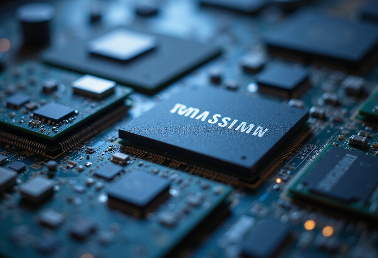
Samsung's LPDDR5X-PIM chip reaches 614 GB/s of internal bandwidth across its 16 banks — roughly eight times the 76.8 GB/s ceiling of conventional DRAM accesses that touch only two banks in parallel. The company presented the design at Hot Chips 2026 as the latest step in its processing-in-memory (PIM) push, placing MAC compute units inside LPDDR5X-9600 chips while preserving compatibility with a standard memory controller.
The core idea exploits a structural fact of DRAM: compute inside a memory chip can use its higher internal bandwidth and avoid the long latency path between DRAM and host compute cores.
How does the design work?
The chip resembles a standard LPDDR5X-9600 part with 16 banks, but each bank gets an attached PIM block. These blocks read their local banks without passing through the chip's constrained external bus.
Each PIM block contains:
- A MAC tree with surrounding register files and control logic
- A 1024-bit instruction register file holding up to 64 16-bit instructions
- A 4 kbit source register file for activation vectors, supplying one MAC operand
- A 2 kbit scale register holding factors applied to model weights before MAC computation
Samsung expects software to load model weights into DRAM, which supplies the second operand directly to the MAC array. The array supports low-precision formats: four INT8 or FP8 MAC operations per data clock, or eight per cycle when excluding double data rate. Throughput doubles with 4-bit input weights, bringing package-wide compute to 2.4 TOPS.
That figure is modest on its own. Eight LPDDR5X-PIM chips together would deliver 9.6 INT8 TOPS — approximately matching the NPU in Intel's Meteor Lake. The cost is substantial, since eight 16 GB chips correspond to 128 GB of system memory.
What does the command interface look like?
LPDDR5X-PIM stays within the standard LPDDR5X protocol while exposing compute features the memory standard does not define. Samsung reserves special row addresses that function like MMIO addresses. Each channel has a pair of predefined rows for mode control: one activation sets single-bank mode, the other sets multi-bank mode, which applies commands across all 16 banks.
Additional special per-bank rows put the chip into PIM Registers Activated mode, where read and write commands target PIM registers instead of DRAM contents. A typical ML workflow loads weights in single-bank mode, switches to multi-bank mode with registers activated, writes activation values and scale factors, and specifies operations in the instruction registers. Because writes broadcast across all 16 banks, PIM behaves like a constrained SIMD processor.
With 256-bit DRAM packets (BL=16), filling each source register takes 16 write commands; doing that bank by bank across 16 banks would require 256 write commands, making host-to-PIM register bandwidth the limiting factor without broadcast.
Samsung also addressed memory-controller reordering. An Address Align Mode (AAM) lets each instruction infer its source register index from the column address being accessed, so reordered accesses cannot break the sequential instruction-to-register mapping.
What breaks for software?
Samsung reports large internal performance gains over standard LPDDR5X, and the design's compatibility with standard memory controllers is a genuine engineering achievement. But the software problems are steep.
Because PIM modes change the meaning of DRAM commands, software cannot mix PIM use with regular memory accesses — even across threads. A non-PIM thread reading memory during PIM operation could trigger unintended computation and corrupt the PIM vector register files. Samsung's answer is for the host to isolate a PIM region in memory, which likely means designating entire channels as PIM-only, at the cost of bandwidth for non-PIM applications and compute for PIM code.
Multitasking operating systems face worse problems. Preempting a PIM thread would require taking the channel out of PIM mode and saving instruction, source, scale, and vector register state across every bank. Handling interrupts and context switches this way places a heavy burden on the OS.
Caches compound the issue. DRAM can generate values the cache hierarchy never sees, and caches can absorb accesses meant to trigger PIM operations. Samsung recommends mapping PIM memory as uncacheable — and PIM reads act like MMIO accesses, so speculative execution, prefetching, and out-of-order loads become hazards. Running without caching, prefetching, or out-of-order execution cripples CPU performance.
Beyond mode switching, each PIM block only has fast access to its local bank. PIM blocks cannot exchange data directly; the host must shuttle results between banks through regular DRAM traffic.
What would make adoption realistic?
The presentation suggests in-memory compute needs changes throughout the memory subsystem rather than clever repurposing of existing commands. Candidate fixes include explicit compute commands in the DRAM interface, a memory controller acting as a cache-coherent peer using read-for-ownership requests, and new CPU instructions that abstract whether compute runs in memory or on the core.
Such changes would let a multitasking OS use in-memory compute without reserved memory regions, uncacheable mappings, or blocked threads. Without them, the tradeoffs around performance, memory capacity, and responsiveness remain difficult to reconcile.
via substackcdn.com (Original)
More from Elena Vasquez
Show full bio
Senior reporter covering people, launches and day-to-day practice in hardware layer of artificial intelligence at Die Signal.
285 articles
Same lot · LOT-C1C6
- DSG-384410nmSamsung's Drop-In DRAM Chip Triples AI Inference Speed
- DSG-995110nmSamsung: HBM to Absorb Nearly 30% of Global DRAM Capacity Next Year
- DSG-75607nmSamsung Forecasts HBM at 30% of DRAM Capacity by 2027
- DSG-502510nmSamsung Exec: HBM to Reach Nearly 30% of Global DRAM Capacity
- DSG-96247nmSamsung to outsource custom DRAM, redirect fabs to HBM for AI