Test report DSG-9974 · Rev A · tested October 14, 2026
Foundries & ManufacturingDevice under test
GlobalFoundries to build two New York fabs under $21bn US-Japan deal
GlobalFoundries will build two 300mm fabs in Malta, New York, under a $21bn US-Japan deal, with Japan funding an initial $10bn tranche and the first fab due online in 2029.
- Read
- 2 min
- Words
- 448
- Node
- 65nm
- Operator
- Marcus Bennett
Spec summary
- GlobalFoundries will build two new fabs at its Malta, New York, site under a $21bn US-Japan deal
- Japan provides an initial $10bn for a 300mm fab slated to come online in 2029
- The two fabs will have combined annual capacity of around 900,000 300mm wafers
- GF will reallocate $995m of its CHIPS Act award into silicon photonics, SiGe and advanced packaging
- The US Commerce Department will receive a four percent equity stake in GF
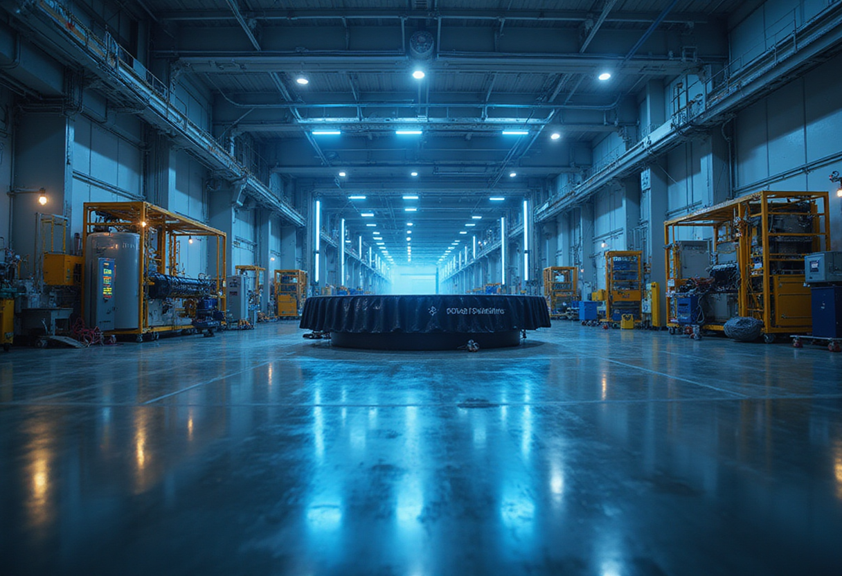
GlobalFoundries will build and operate two new fabs in Malta, New York, under a $21 billion US-Japan semiconductor initiative. Japan provides the investment. The first $10 billion tranche funds a new 300mm fab slated to come online in 2029.
The site of the first fab is permitted and "shovel-ready," according to GF. The company expects to break ground later this year. A second $10 billion investment package would then fund a second fab, adding what GF calls "significant new US manufacturing capacity" to support its global customer base.
What do the two fabs deliver?
Combined, the facilities will have an annual production capacity of around 900,000 300mm wafers. GF puts the jobs figure at approximately 27,000 construction and ecosystem jobs, plus more than 1,000 high-skilled manufacturing jobs around New York City.
The mechanism is straightforward: Japanese capital, American manufacturing capacity, GF as operator. The deal adds a second leg. GF and the US Department of Commerce agreed to amend GF's existing CHIPS and Science Act award, reallocating $995 million into silicon photonics, silicon-germanium (SiGe) and advanced packaging at its Malta, New York, and Burlington, Vermont, facilities.
Under a separate agreement, the US Department of Commerce will receive a four percent equity stake in GF.
Why GF?
CEO Tim Breen framed the selection around capability, not just capital. "This is a bold new initiative for semiconductor manufacturing, bringing together the United States and Japan with GF's differentiated technology and decades of manufacturing expertise to accelerate trusted capacity in New York," Breen said.
He added: "GF was selected because fabs of this scale require more than capital. They require differentiated technology, operational excellence, and a proven ability to execute. That combination is what positions GF to make this first-of-its-kind initiative a success."
Secretary of Commerce Howard Lutnick tied the deal to broader trade policy. "President Trump's historic US-Japan Trade Deal is delivering another massive manufacturing investment into America," Lutnick said. "With Japan's investment funding and GlobalFoundries' partnership, two large semiconductor chip manufacturing facilities will be built in the US, creating thousands of high-paying jobs for American workers."
What does this change for GF's customers?
More capacity, on a defined timeline. The first fab comes online in 2029 with the second following, and the CHIPS award amendment pushes GF's Malta and Vermont sites toward silicon photonics, SiGe and advanced packaging — technologies relevant to optical interconnect and RF markets. The Commerce Department's four percent stake also signals a direct federal interest in GF's execution.
The Malta expansion adds to GF's existing footprint at the site. Groundbreaking is expected later this year.
via Data Center Dynamics (Source)
More from Marcus Bennett
Show full bio
News editor covering regulation, policy and their impact on hardware layer of artificial intelligence at Die Signal.
369 articles
Same lot · LOT-C1CA
- DSG-723714nmUp To $21 Billion U.S.-Japan Plan Puts Two New York Fabs Under GlobalFoundries
- DSG-58987nmGlobalFoundries picked to run two new fabs in Malta, N.Y.
- DSG-52947nmGlobalFoundries Picked to Run Two New York Fabs Under U.S.-Japan Plan
- DSG-970365nmGlobalFoundries Picked to Run Two New Malta Fabs Under US-Japan Plan
- DSG-875820nmGlobalFoundries Plans New York Fab Worth Up to ¥3.3 Trillion