Test report DSG-5373 · Rev D · tested October 13, 2026
AI Datacenter InfrastructureDevice under test
Enteligent unveils three-stage 800VDC-to-chip power stack for AI racks
Enteligent has unveiled a three-stage power architecture that takes 800 volts DC at the rack input and converts it all the way down to chip-level voltage, aimed at AI training and inference racks where 48V distribution no longer scales.
- Read
- 3 min
- Words
- 581
- Node
- 10nm
- Operator
- Elena Vasquez
Spec summary
- Enteligent unveiled a three-stage 800VDC-to-chip power stack targeting AI training and inference racks.
- Modern rack densities are pushing past 50 kilowatts per unit and heading toward 100-plus, beyond what 48-volt DC distribution was designed for.
- An 800VDC bus can deliver the same power as a 48VDC bus at roughly 1/16th of the current - 1,000 amps drops to about 60 amps.
- Most current 800VDC designs stop at the rack; Enteligent's three-stage stack collapses two intermediate steps into the rack-level hardware.
- Efficiency curves, named reference designs, pricing, and safety certification timing have not yet been disclosed.
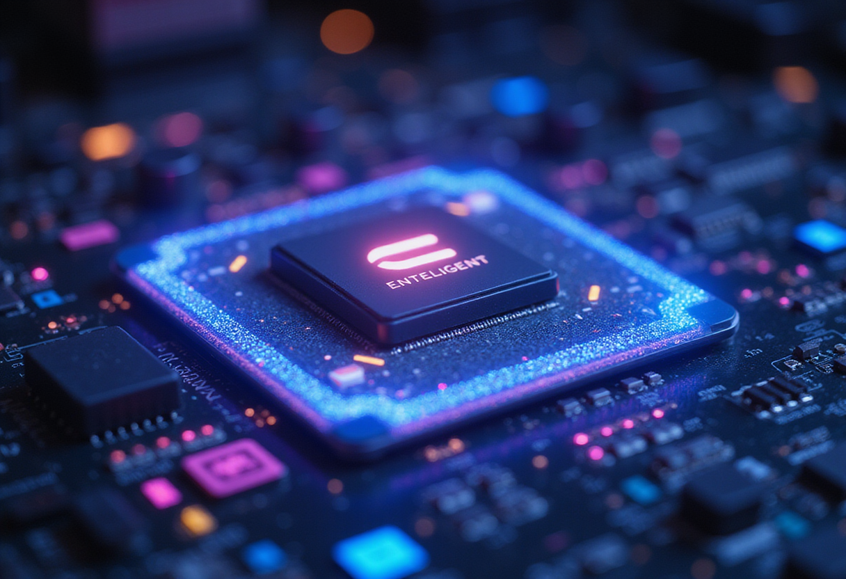
Enteligent has unveiled a three-stage power architecture designed to take 800 volts DC at the rack input and convert it all the way down to the voltage silicon actually uses, targeting AI training and inference racks.
The product lands in a category every hyperscale operator is currently scrutinizing. As rack densities push past 50 kilowatts per unit and head toward 100-plus, the legacy 48-volt DC distribution scheme starts to break down: currents get punishing, copper gets heavy, and conversion losses eat into the power budget before any compute happens.
The "three-stage" label is the key differentiator from what most of the broader industry is currently pursuing. Most 800VDC designs stop at the rack and hand 48 volts off to the existing point-of-load regulators on the server board, which then finish the trip down to roughly 0.8 volts at the die through multiple VR phases.
Enteligent's pitch, by collapsing two of those intermediate steps into the rack-level stack, is fewer conversion stages on the GPU board, less energy burned as heat, and more PCB real estate available for compute and memory.
Why does 800VDC matter for AI racks?
The arithmetic is straightforward. Power equals voltage times current, so doubling the distribution voltage cuts the current in half at the same power. Copper cross-section scales with current, so the savings compound.
A 48VDC bus carrying 1,000 amps drops to roughly 60 amps on an 800VDC bus for the same load. That's the difference between finger-thick busbars and cables thick as a wrist - and a meaningful reduction in cooling overhead for the distribution path itself.
The major cloud operators have all been signaling movement toward high-voltage distribution over the past 18 months. The drivers aren't efficiency alone; the bigger prizes are standardization across global fleets, simpler mechanical designs, and the headroom to push rack densities past what 48VDC was ever designed to handle.
What changes for practitioners if this lands?
If Enteligent's stack delivers what the architecture implies, a data center operator could simplify server-board design, shrink the VR footprint, and reclaim PCB area for compute. Every percentage point of efficiency saved at the rack level translates into meaningful operating cost over a multi-year fleet deployment.
For colocation providers running mixed-tenant floors, the calculus is different. They don't control the server SKU inside every cage, which means any rack-level power stack has to be flexible enough to feed the diverse silicon a colo sees - Nvidia today, possibly a custom ASIC tomorrow.
That's why the announcement matters even without a full datasheet. The direction of travel - high voltage from grid to gate - is settled across the industry. The open question is who defines the rack-level stack between the bus and the chip.
What's missing from the announcement?
The disclosure leaves several questions unanswered. The company has not published efficiency numbers at the typical 50% or 100% load points that procurement teams ask for first. It hasn't named a specific GPU or accelerator reference design, disclosed pricing, or given a certification timeline.
By press time, Enteligent had not responded to requests for comment on those specifics.
For practitioners planning 2026 or 2027 AI cluster builds, the watch items are clear: a public efficiency curve, a reference design with a named accelerator partner, and a certification timeline. Those three pieces turn an architecture announcement into something a procurement team can actually evaluate.
via Google News: GPU datacenter (Source)
More from Elena Vasquez
Show full bio
Senior reporter covering people, launches and day-to-day practice in hardware layer of artificial intelligence at Die Signal.
306 articles
Same lot · LOT-C1C9
- DSG-456728nmGoogle, Microsoft and Nvidia Back 800V DC Standard for AI Data Centers
- DSG-68715nmABB Ships Infinitus: First Source-to-Rack 800VDC Portfolio for AI Data Centers
- DSG-18625nmInfineon to supply Eaton SiC devices for 800VDC data center power
- DSG-55275nmCisco and Nvidia target enterprise AI with rack-scale systems
- DSG-294245nmMicrosoft's Maia 300: 96 Chips, 167 kW, 40% More Tokens Per Watt