Test report DSG-8037 · Rev B · tested October 10, 2026
AI Datacenter InfrastructureDevice under test
d-Matrix Puts AI Compute Die on Custom DRAM, Hits 100 TB/s
At Hot Chips 2026, d-Matrix detailed an AI accelerator that bonds a TSMC 4nm compute die face-to-face onto custom DRAM at 36-micron pitch, reaching 100 TB/s per card.
- Read
- 3 min
- Words
- 568
- Node
- 3nm
- Operator
- Marcus Bennett
Spec summary
- d-Matrix claims 100 TB/s memory bandwidth per card
- Compute die manufactured on TSMC 4nm process
- Face-to-face die bonding at a 36-micron pitch
- Memory is a custom-designed DRAM die, not standard HBM
- Architecture disclosed at Hot Chips 2026
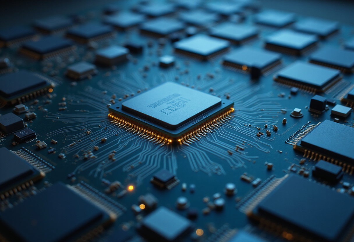
d-Matrix has presented an AI accelerator architecture that delivers 100 TB/s of memory bandwidth per card by stacking the compute die directly on top of custom-designed DRAM, according to details disclosed at Hot Chips 2026.
The design bonds a TSMC 4nm compute die face-to-face onto a custom memory die at a 36-micron bump pitch. That direct vertical connection replaces the long interposer traces and package-level signaling that constrain conventional GPU-to-HBM designs.
Why 100 TB/s per card matters
Memory bandwidth, not raw FLOPS, now limits inference performance on large models. Serving transformer-based workloads is dominated by the movement of weights and key-value caches between memory and compute. By placing the accelerator die in physical contact with the DRAM it reads from, d-Matrix shortens that path to a stack of microscopic bonds.
The 100 TB/s figure is a per-card aggregate. It positions the architecture against conventional HBM-based cards, where the memory controller, package substrate and interconnect consume both bandwidth headroom and power budget.
What does the face-to-face bonding change?
Three specifications define the approach:
- TSMC 4nm process for the compute die — a mature, high-yield node chosen over leading-edge lithography.
- 36-micron bonding pitch between the two dies, an aggressive density for face-to-face attachment.
- Custom-designed DRAM die rather than an off-the-shelf HBM stack, which lets d-Matrix tune the memory's organization to the accelerator's access patterns.
Face-to-face bonding means the active surfaces of both dies meet directly. Signals cross through micro-bumps instead of traveling through package routing. The result is a shorter, wider, lower-power channel between logic and memory — the property that enables the quoted bandwidth figure.
Building a custom DRAM die is the costlier part of the equation. Standard HBM benefits from volume manufacturing across many customers; a bespoke memory die serves one architecture. d-Matrix is betting that the inference market's sensitivity to bandwidth justifies that dedicated silicon.
A different bet than the GPU incumbents
The mainstream response to the memory wall has been to widen HBM interfaces and add more stacks per package. d-Matrix instead changes the physical relationship between compute and memory: the accelerator sits on the memory, not beside it.
The choice of TSMC 4nm signals a deliberate trade. Leading-edge nodes buy density and clock speed for training-class silicon; inference at the edge of the memory system rewards I/O density and yield economics more than peak logic performance.
What remains open
The Hot Chips 2026 disclosure specifies the interconnect, process node and bandwidth target. Card-level power draw, memory capacity per stack, production timing and pricing were not part of the headline figures.
Those gaps matter for deployment planning. A 100 TB/s card only translates into throughput if the memory capacity holds the target models and the power envelope fits rack-level constraints. d-Matrix will need to publish capacity and thermal data before data-center buyers can benchmark the architecture against HBM-based alternatives on a per-watt basis.
For now, the numbers on the table are concrete: TSMC 4nm compute logic, a purpose-built DRAM die, a 36-micron face-to-face bond, and 100 TB/s per card. That combination marks one of the most aggressive logic-on-memory integrations shown at the conference to date.
via Google News: DRAM chip (Source)
More from Marcus Bennett
Show full bio
News editor covering regulation, policy and their impact on hardware layer of artificial intelligence at Die Signal.
314 articles
Same lot · LOT-C1C6
- DSG-995110nmSamsung: HBM to Absorb Nearly 30% of Global DRAM Capacity Next Year
- DSG-58745nmNvidia unveils custom high-bandwidth memory, but allocation stays unclear
- DSG-109114nmChinese AI Chipmakers Lift Prices as HBM Shortage Tightens Supply
- DSG-161214nmAI Demand for HBM Pushes Ordinary RAM Prices Above Cutting-Edge Chips
- DSG-30563nmHuang's '2x Chip Vow' Reserves 37% of HBM Supply Through 2026