Test report DSG-5915 · Rev B · tested October 13, 2026
Memory & StorageDevice under test
China Builds First 3.5D 'Infinity Chiplet' and 3D DRAM to Bypass HBM Squeeze
China's first 3.5D 'Infinity Chiplet' packaging and domestic 3D DRAM target the HBM bottleneck squeezing its AI supply chain.
- Read
- 2 min
- Words
- 431
- Node
- 45nm
- Operator
- Elena Vasquez
Spec summary
- China has developed its first 3.5D 'Infinity Chiplet' packaging technology.
- The program pairs chiplet integration with domestic 3D DRAM to substitute for restricted HBM.
- The effort targets the memory-bandwidth bottleneck in China's domestic AI supply chain.
- Export controls on HBM access are the driving constraint behind the development.
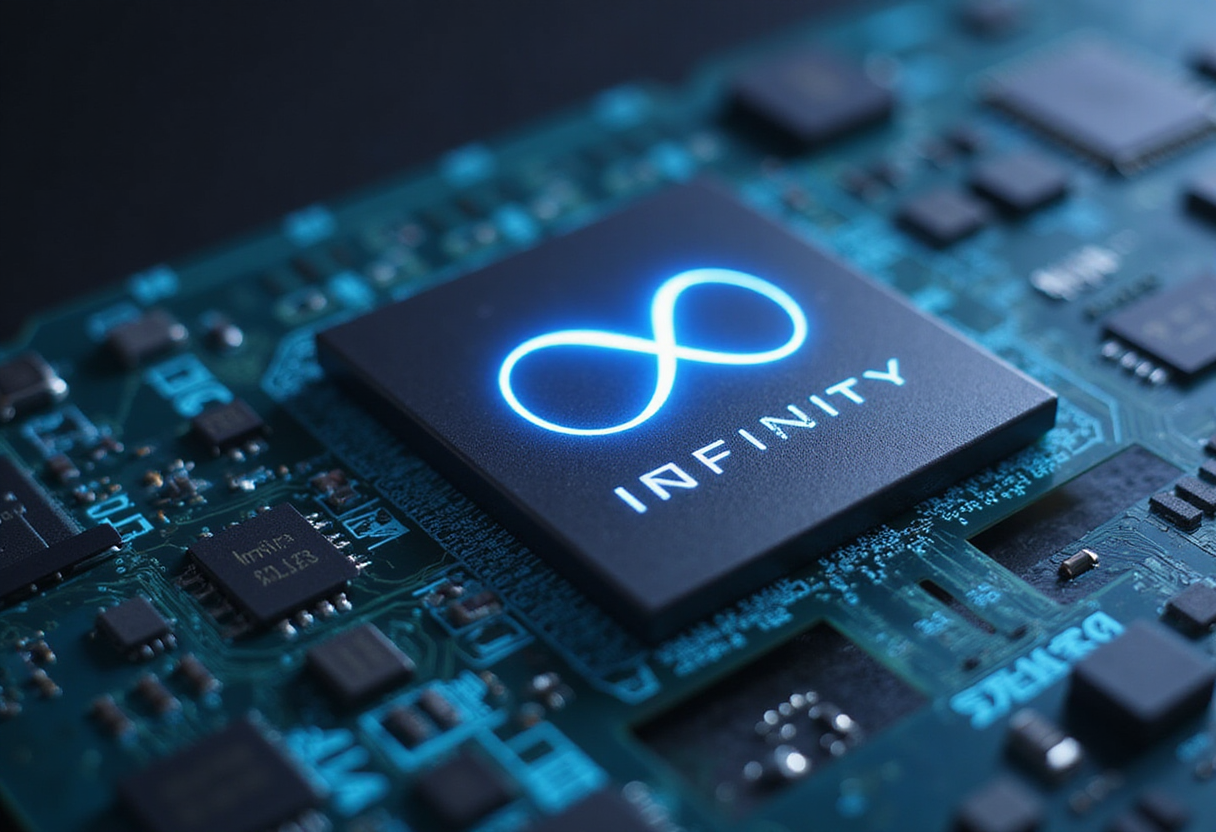
China has developed its first 3.5D "Infinity Chiplet" packaging technology alongside domestic 3D DRAM, a pairing aimed squarely at the memory bottleneck constraining its AI accelerator pipeline, Wccftech reports.
The move matters because high-bandwidth memory — HBM — has become the choke point for anyone building AI silicon. Export controls limit Chinese firms' access to leading HBM supplies, so the country's answer is to work around the constraint rather than through it.
What is 3.5D packaging actually doing?
Chiplet packaging splits a large monolithic GPU-class die into smaller pieces and stitches them back together on an interposer or substrate. The "3.5D" label refers to stacking and side-by-side integration combined — dies placed both laterally and vertically, shortening the distance data has to travel.
For practitioners, the practical payoff is bandwidth-per-square-millimeter. If you can't buy the fastest HBM on the open market, you compensate by shortening the copper between compute and memory. That's the engineering logic here.
Why pair it with 3D DRAM?
HBM is the standard answer for feeding AI accelerators, and China's access to it is constrained. Domestic 3D DRAM — memory stacked in layers rather than spread flat — is the substitute path.
Stacked DRAM placed close to, or on top of, compute chiplets changes the memory equation. You trade the peak bandwidth of top-tier HBM for proximity and supply security. For a national AI program that can't rely on foreign vendors, that trade is the whole point.
What does this change for the AI supply chain?
A few concrete implications:
- Chinese accelerator designers get a domestic route to memory bandwidth, reducing exposure to export controls on HBM.
- Packaging — historically a commoditized step — becomes the strategic layer, since 3.5D integration can offset some of what's lost on the memory side.
- Western vendors now face a competitor that's vertically motivated: every constraint applied externally accelerates investment in the workaround.
The bigger picture
The "Infinity Chiplet" branding echoes how the industry talks about interconnect-first design — AMD's approach with its own chiplet architecture comes to mind as the reference point practitioners will reach for.
Whether Chinese 3D DRAM can match leading HBM generations on bandwidth and power efficiency remains the open question. Wccftech's report describes the development as a first — meaning volume production, yields and real-world accelerator performance are still ahead.
Still, the direction is clear. China is treating memory bandwidth not as a component to procure but as a capability to build, and packaging is where it's choosing to make its stand.
via Google News: DRAM chip (Source)
More from Elena Vasquez
Show full bio
Senior reporter covering people, launches and day-to-day practice in hardware layer of artificial intelligence at Die Signal.
320 articles
Same lot · LOT-C1C9
- DSG-156365nmHouse CCP Committee Presses Commerce on DRAM, AI Chip Licensing
- DSG-109114nmChinese AI Chipmakers Lift Prices as HBM Shortage Tightens Supply
- DSG-751765nmCXMT Puts $5.2 Billion Behind DRAM Expansion, Backing Chinese Toolmakers
- DSG-618728nmCXMT DRAM Reaches Market but Undercuts No One on Price
- DSG-40957nmSK Hynix Taps Intel EMIB-T for Next-Gen HBM Packaging